Wireless EV Charger Communication PCB Can Fd / PLC Interface for ISO 15118 Compliant Smart Charging Station UL & CE Certified

Still deciding? Get samples of $ !
Request Sample

Product Description

Technical Specifications
Model NO.
pcb
Material
Fiberglass Epoxy
Application
Communication
Flame Retardant
V0
Mechanical Rigid
Rigid
Base Material
Fr4 Tg150
Board Thickness
Customized
Copper Thickness
1 Oz
Max PCB Size
650*650mm
Surface Finishing
Enig
Lead Time
4-5 Working Days
Compliance
RoHS, ISO9001, UL, SGS
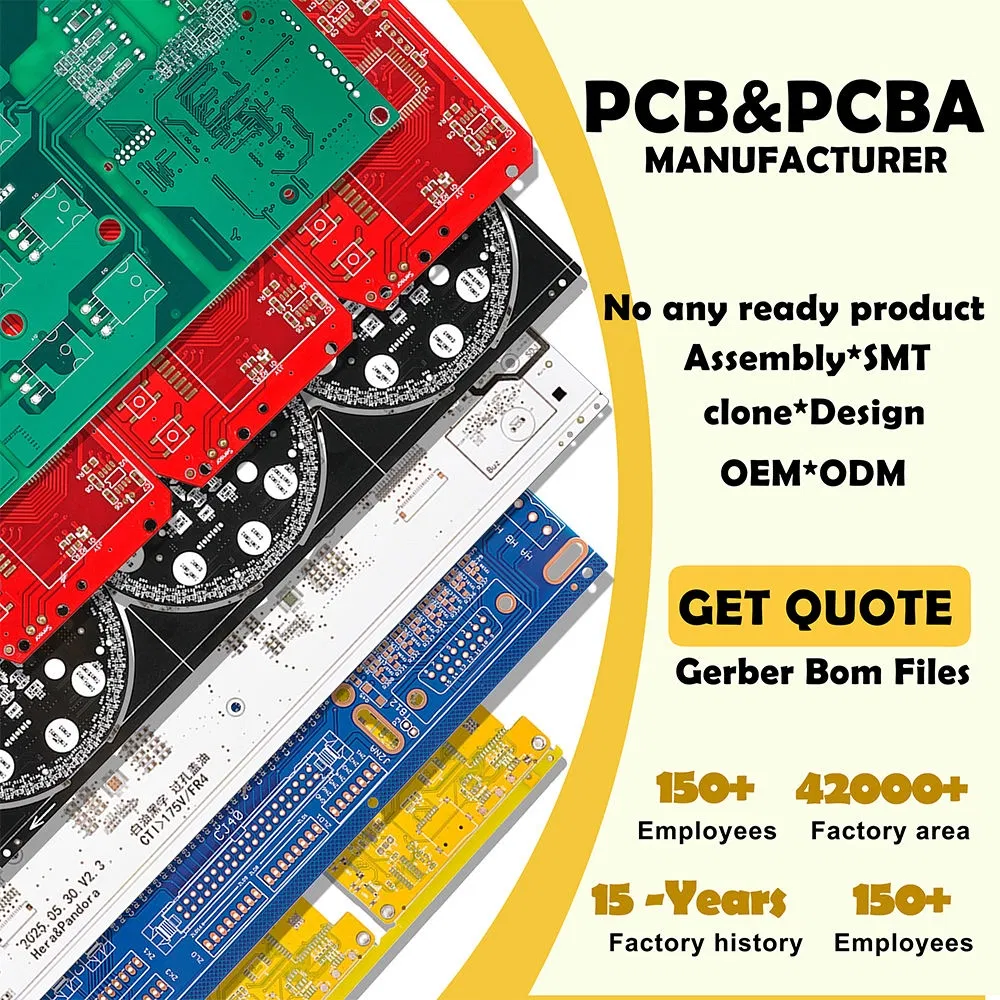
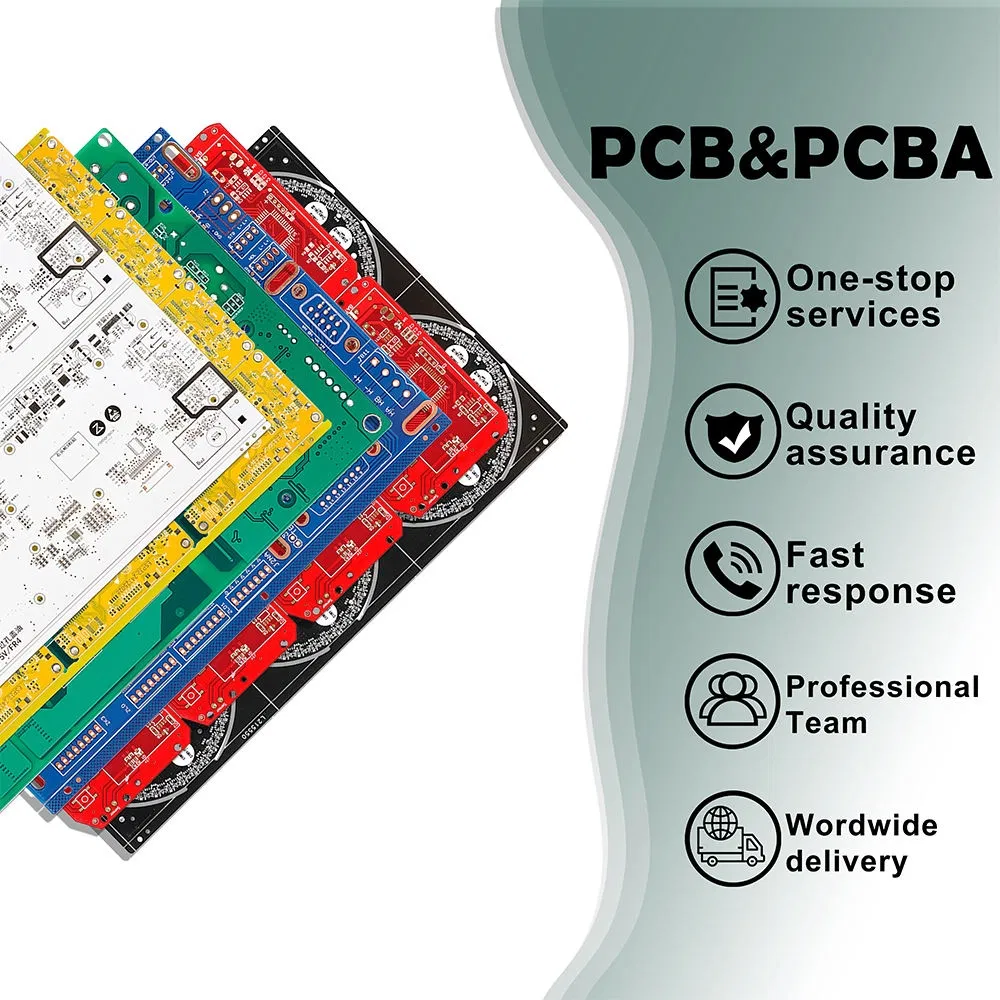
Product Presentation
PCB Communication Interface Smart Charging Station PCB ISO 15118 Compliant PCB
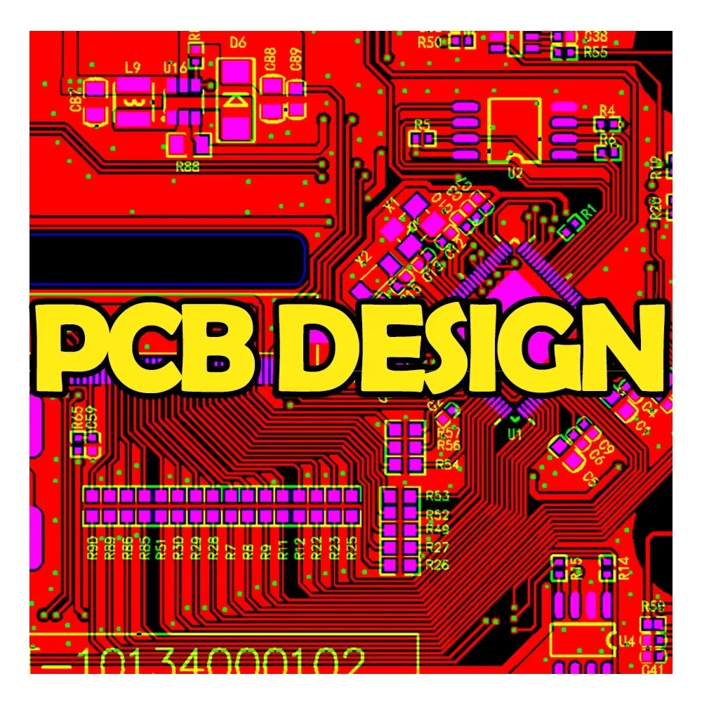
Professional PCB Fabrication Services

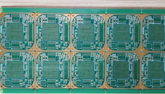
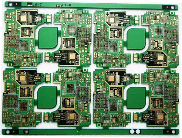
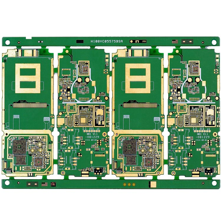
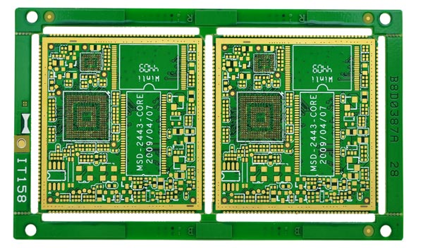
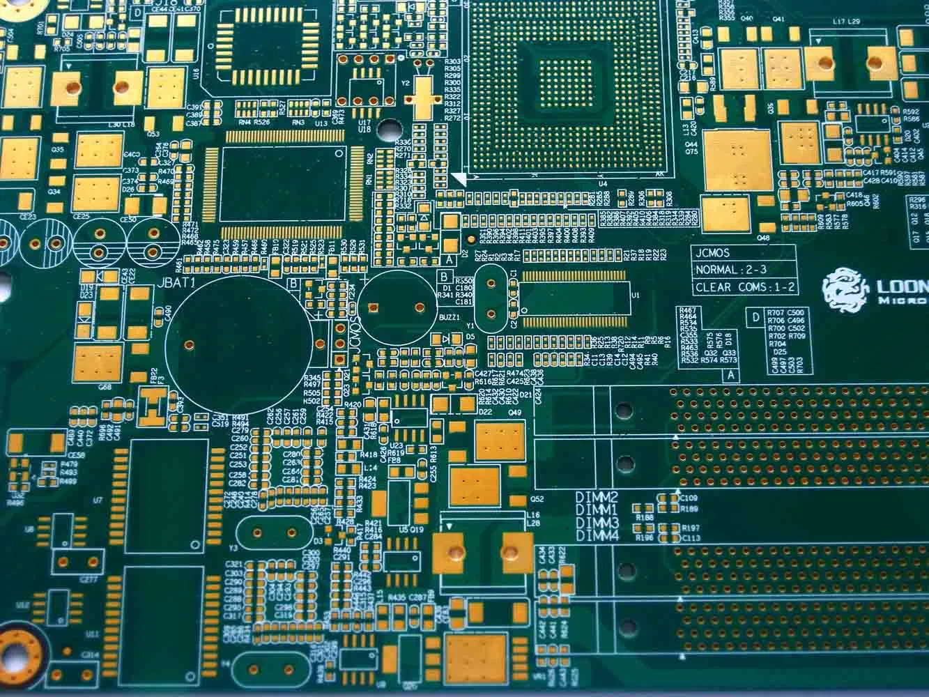
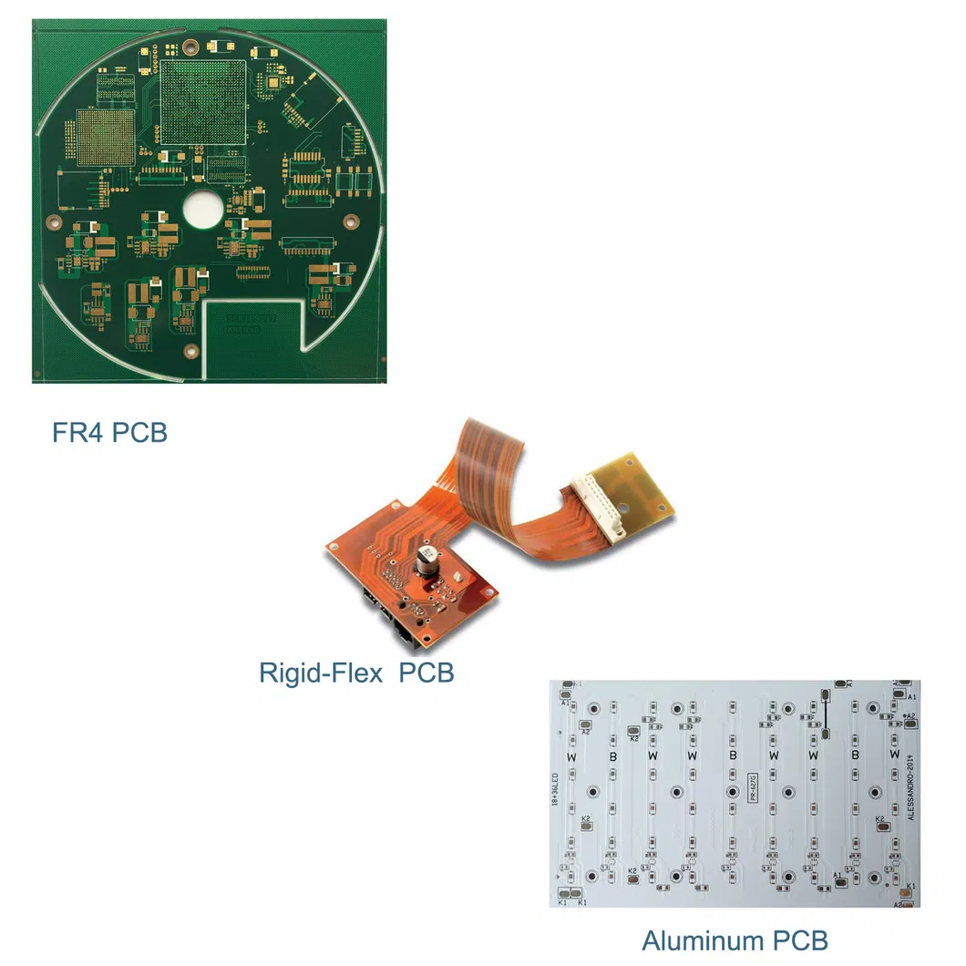
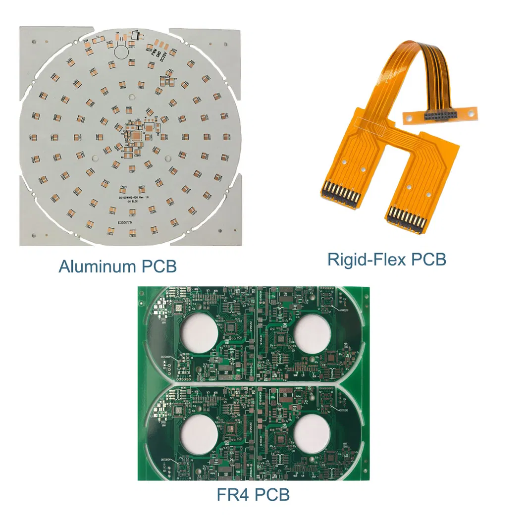
Providing high-precision 1-26 layers PCB board solutions including design, fabrication, clone, and assembly services with UL, ISO, and SGS certifications.

Our Production Range
  • Single & Double Side PCB
  • Multilayer PCB (up to 26+ layers)
  • Flexible PCB (FPC) & Rigid-flex
  • Aluminum & Metal Core PCB
  • Ceramic & HDI PCB Boards
  • High Frequency PCB Solutions
  • Complete PCB Assembly (PCBA)
  • MCPCB for LED Applications
PCBA Manufacturing Capabilities
Feature Specifications
Assembly TypesTHD, SMT, Mixed SMT & THD, 2-sided assembly
SMT Line Quantity30 Lines
Smallest Components01005
BGA Min Pitch0.25mm
Board ShapeRectangular, Round, Complex, Irregular
Testing ProceduresVisual, X-ray, AOI, ICT, Functional Testing
PCB Technical Capabilities
Parameter Capability
Material TypesFr-4, Fr-5, High-Tg, Halogen Free, Rogers, Isola, Teflon, Aluminum/Copper Based
Min. Track Width/Space3mil / 0.075mm
Internal Cu ThicknessHOZ-8OZ
Laser Drilling Size4mil / 0.1mm
Solder Mask ColorGreen, Blue, White, Black, Red, Yellow, Purple, etc.
Surface FinishingHASL, Lead Free HASL, Immersion Gold/Tin/Silver, OSP, Hard Gold
Prototype Lead Time
Layers General Time Quick Turn
1-2 Layers4 Days1 Day
4-6 Layers6 Days2 Days
8-10 Layers8 Days3 Days
12-16 Layers12 Days4 Days
18-26 Layers14-16 Days5-6 Days
Manufacturing Facility
Factory Overview
Production Line Testing Area Equipment
Quality Control
Frequently Asked Questions
Q1: Are you a factory or a trading company?
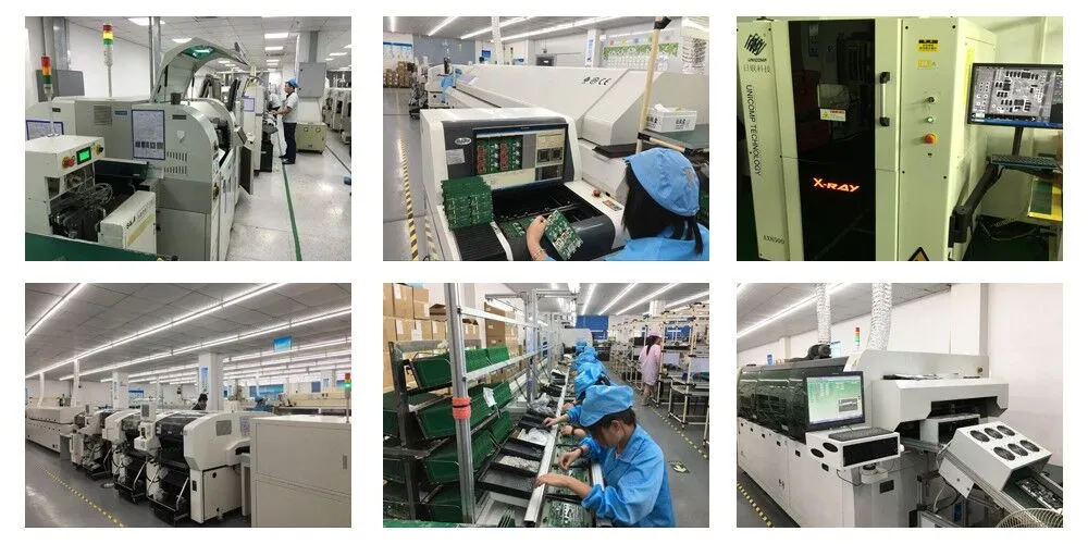
We have our own specialized PCB manufacturing and assembly factory to ensure quality control and competitive lead times.
Q2: What is your minimum order quantity (MOQ)?
We have no MOQ. We welcome both small prototype orders and large-scale production runs.
Q3: What files are required for a quotation?
For PCB, Gerber files are preferred (Protel, Power PCB, PADs). For PCBA, please provide Gerber files along with a detailed BOM (Bill of Materials).
Q4: Can you produce PCBs from a physical sample if I have no Gerber files?
Yes, we can help you clone the design. Just send the physical sample to us, and our engineers will work out the design files for production.
Q5: What are your standard delivery terms and times?
We usually use FOB terms. Delivery typically ranges from 7 to 30 days depending on the order quantity, complexity, and specific customization requirements.
Q6: What testing procedures do you use for quality assurance?
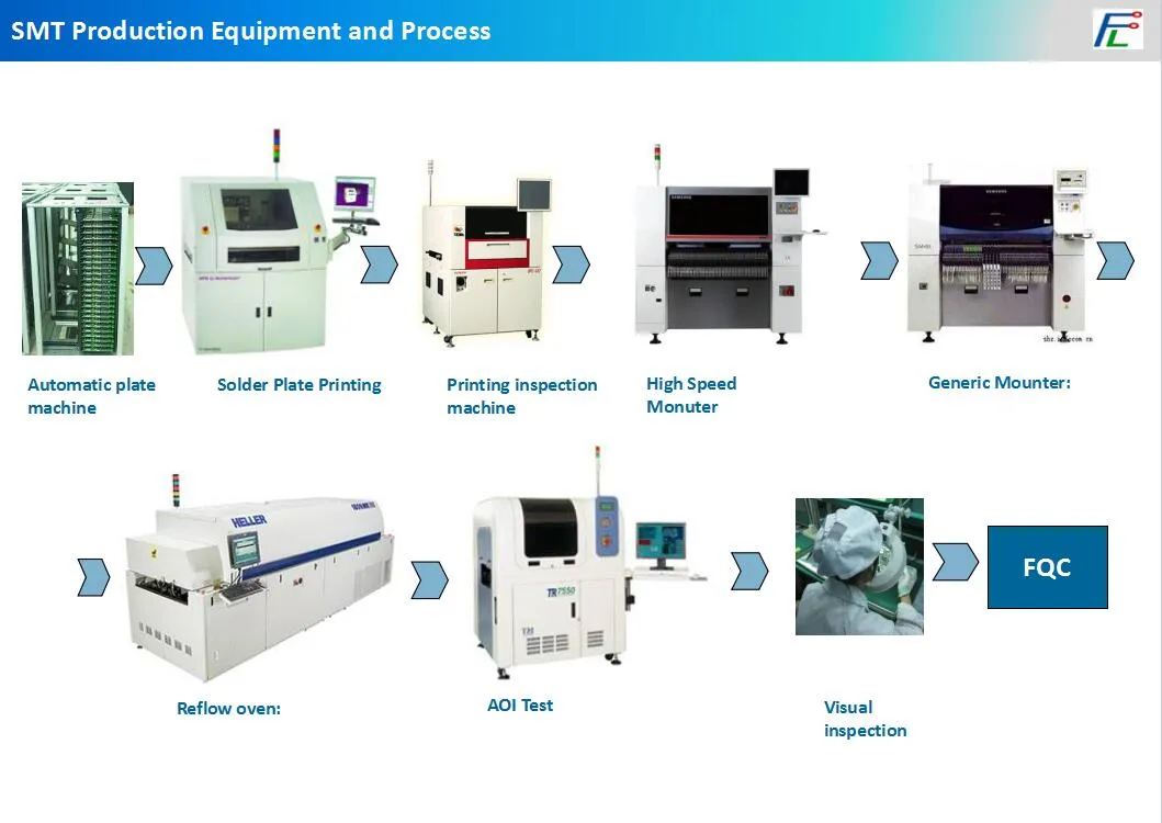
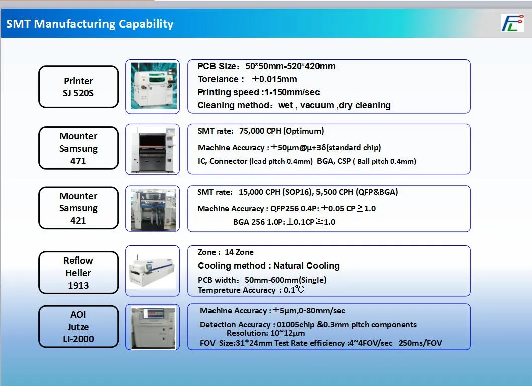
We employ multiple testing stages including Visual Inspection, AOI (Automated Optical Inspection), X-ray Inspection for BGA, and Functional Testing to ensure zero-defect delivery.

Related Products